Understanding the core distinction between EMI and EMC is the secret to developing stable, globally compliant electronic systems. While EMI is the physical electromagnetic noise leaving a device, EMC is the design standard that ensures your product coexists safely within its operating environment.
Sourcing electronic components often comes to a grinding halt due to unexpected high-frequency electrical noise. This interference can corrupt your signal integrity, trigger costly compliance failures, and delay your global product launch by several months. Selecting a high-quality, pre-certified power adapter EMI and EMC solution resolves these critical development bottleneck challenges instantly.
What do power adapter EMI and EMC actually mean?
Understanding power adapter EMI and EMC principles is vital for any hardware engineer integrating power supplies. Electromagnetic interference (EMI) is the physical, unwanted noise generated by high-frequency switching circuits that leaks into surrounding copper lines or the open air. In contrast, electromagnetic compatibility (EMC) is a device’s capability to run correctly in its electromagnetic environment without causing or receiving interference.
What is the physical nature of EMI?
To design a clean system, you must first understand how electromagnetic noise originates and travels. Fast-switching currents generate electrical and magnetic waves that find leakage paths into adjacent wires or escape as radiated energy.
Look:
This energy travels downstream, easily disrupting sensitive digital signals and analog sensors.
- Conducted noise emissions travel directly through copper power cables.
- Radiated noise waves propagate through the air as electromagnetic fields.
- Common-mode noise signals flow in the same direction on power lines.
Why does EMC matter for your product?
Earning international market approval requires your hardware to meet strict, legal electromagnetic boundaries. Achieving EMC means your finished product restricts its active noise emissions while maintaining high immunity to incoming external noise.
Here is why:
Failing a single EMC test will completely halt your product release.
- Limit active emissions to keep your surroundings electrically clean.
- Boost RF immunity to survive harsh external wireless interference.
- Provide ESD protection to prevent system resets from physical contact.
Key Takeaway: EMI is the physical noise problem you must actively suppress, while EMC represents the legal regulatory standard your system must satisfy.
| Metric | Electromagnetic Interference (EMI) | Electromagnetic Compatibility (EMC) | |
|---|---|---|---|
| Physical Nature | Active electrical noise pollution | System coexistence capability | |
| Transmission Vector | Cables and open-air radiation | Filtering, shielding, and immunity | |
| System Goal | Minimize or eliminate signals | Comply with legal global limits |
Engineers must analyze these distinct transmission characteristics to build effective multi-stage filter networks that block interference paths.
Why care about power adapter EMI and EMC impacts?
Ignoring power adapter EMI and EMC properties during the component sourcing phase is a primary cause of system-level product failure. High-frequency noise can couple directly into downstream processors, corrupting sensitive communication buses and ruining analog signal measurements.
Can noise ruin your signal integrity?
When you integrate a noisy adapter, high-frequency harmonics directly distort your system’s critical DC voltage rails. This unwanted distortion can corrupt digital communication lines or introduce audible background static in audio systems.
Think about it:
A single uncertified power component can ruin your entire user experience.
- Ruins analog calibration by introducing voltage drift in sensors.
- Spikes digital jitter which triggers packet loss in networking gear.
- Causes audible buzzing in sensitive communications and media devices.
How does compliance protect your market?
Sourcing pre-certified power modules is the most effective way to protect your business from costly compliance failures. Testing your system with an uncertified adapter introduces massive risks that can delay your shipping dates by several months.
Here is the catch:
Customs authorities will seize shipments lacking correct international regulatory markings.
- Avoid severe fines by meeting regional regulatory expectations.
- Bypass customs blocks by showing certified compliance stamps.
- Reduce testing costs by using pre-approved sub-assemblies.
Key Takeaway: Prioritizing compliance early in the design cycle prevents unexpected product redesign costs and guarantees clean system power.
| Industry Sector | Typical Noise Vulnerability | Operational Failure Risk | |
|---|---|---|---|
| Medical Devices | RF noise on sensor probes | Corrupted patient monitoring data | |
| Smart Home | Wi-Fi antenna RF saturation | Intermittent wireless offline states | |
| CCTV Security | Video line signal noise | Screen static and horizontal lines |
System integrators should select their power supplies based on these specific industry risks to prevent operational failures.
How does noise affect power adapter EMI and EMC?
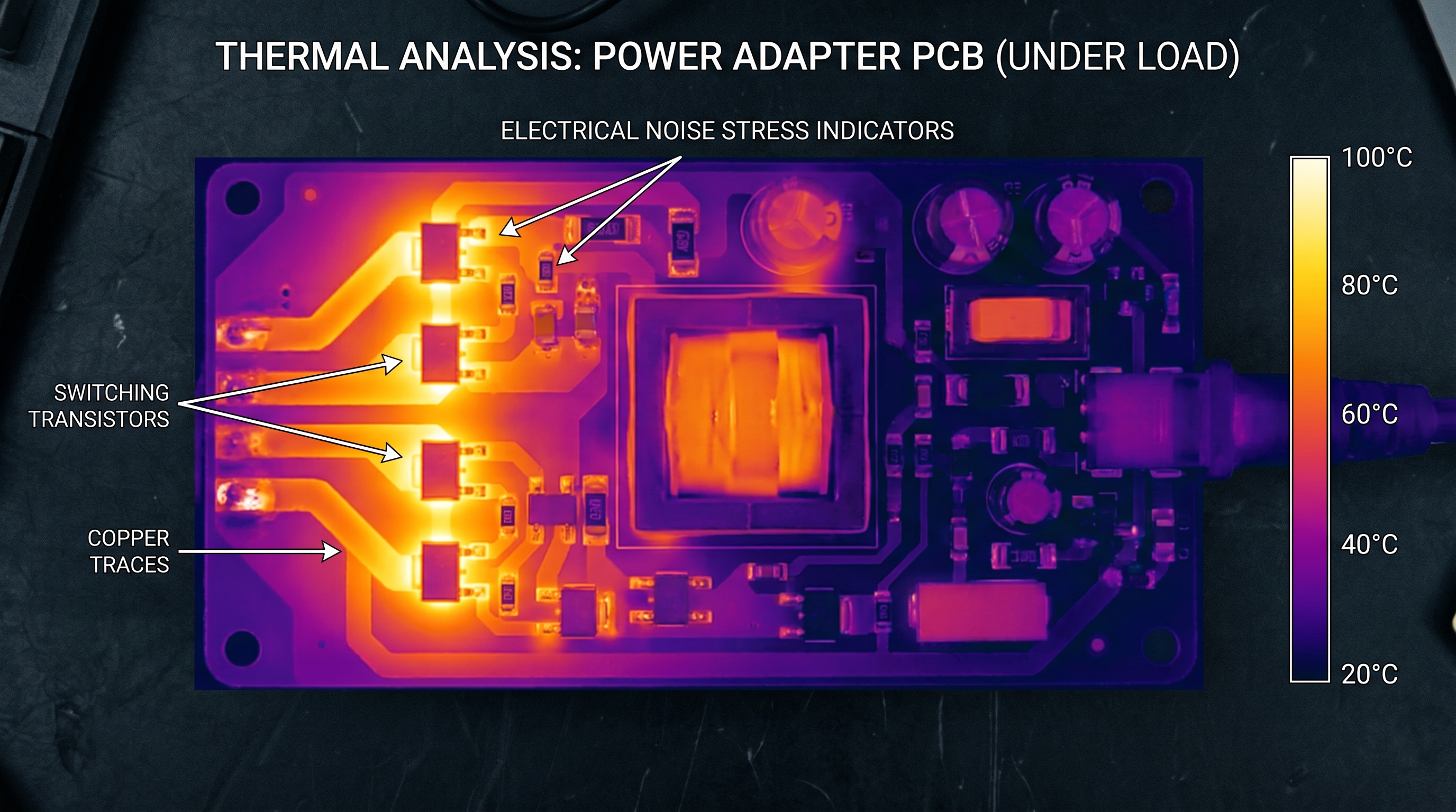
Internal electrical noise does more than disrupt surrounding systems; it directly degrades power adapter EMI and EMC parameters by stressing the internal circuit elements of the adapter. High-frequency parasitics generate localized hot spots and alter the behavior of sensitive semiconductor controllers.
Does noise cause thermal stress?
High-frequency switching transients produce substantial switching losses within the adapter’s primary power transistors. This wasted energy dissipates as intense, localized heat, rapidly driving up component temperatures.
Let’s dive right in:
Excessive operating heat is the primary cause of switching transformer failures.
- Dries out capacitors by accelerating electrolyte wear and evaporation.
- Degrades magnetic cores as temperatures approach material Curie points.
- Lowers conversion efficiency by increasing transistor channel resistance.
Can noise compromise voltage stability?
When high-frequency switching noise couples into the analog feedback loop, the internal controller loses its regulation precision. This results in output voltage ripple, ripple jitter, and sluggish transient responses.
Look at this:
Your downstream processor can crash randomly due to sudden voltage sags.
- Increases output ripple beyond the device’s design limits.
- Slows transient recovery during rapid system load shifts.
- Causes unstable oscillations by eroding the controller’s phase margin.
Key Takeaway: Suppressing internal high-frequency noise protects the power adapter from thermal damage and maintains clean, stable voltage output.
| Critical Component | Internal Noise Vector | Long-Term Reliability Threat | |
|---|---|---|---|
| Electrolytic Capacitors | High ripple current heating | Venting or catastrophic capacity loss | |
| Primary Power MOSFETs | High-frequency voltage spikes | Thermal runaway and gate breakdown | |
| Feedback Optocoupler | Parasitic noise path coupling | Jittery output voltage regulation |
Hardware engineers must manage these component-level stress vectors to design robust, long-lived power supply systems.
What causes major power adapter EMI and EMC issues?
The root source of electromagnetic emissions in any modern switch-mode power supply is the high-speed switching action of its transistors. Analyzing how these switching transitions generate power adapter EMI and EMC problems is crucial to resolving noise failures.
Why does fast switching create noise?
To achieve high efficiency, power adapters switch internal transistors on and off millions of times per second. This rapid change in voltage and current over time inherently creates massive harmonic energy.
Here is why:
These fast switching edge rates generate high-frequency radio waves.
- Rapid voltage changes drive capacitive noise current leakage.
- Fast current transitions produce inductive voltage ringing spikes.
- Diode recovery currents create high-frequency noise on power rails.
How does bad PCB layout leak noise?
Even when utilizing top-tier components, a poorly optimized PCB layout acts like an active radio transmitter. Large current trace loops behave as highly efficient antennas that radiate noise into your system.
Look:
Keeping high-frequency switching paths physically tight prevents this radiation.
- Large loop areas which maximize radiating magnetic field lines.
- Overlapping dirty traces which couple noise directly to clean wires.
- Shared ground tracks which introduce common-impedance coupling paths.
Key Takeaway: Stopping electromagnetic noise at the source through tight layout routing is far cheaper than applying heavy shielding later.
| Noise Source | Physical Mechanism | Primary Prevention Method | |
|---|---|---|---|
| Radiated Loop | Large switching trace loops | Route tracks closely over ground planes | |
| Conducted Spikes | Rectifier reverse recovery | Implement RC snubber bypass networks | |
| Common-Mode | Interwinding capacitance | Install shield plates in the transformer |
PCB layout artists must prioritize minimizing switching loop trace dimensions to suppress radiated noise emissions.
Can shielding solve power adapter EMI and EMC?
When internal filters cannot suppress radiating energy sufficiently, applying physical barriers becomes your next line of defense. Utilizing strategic metal shielding is an excellent way to contain power adapter EMI and EMC radiated fields.
How do metal enclosures block fields?
A conductive metal shield surrounding the power supply board acts as a protective Faraday cage. It absorbs and reflects radiating magnetic and electrical fields, keeping them trapped inside the casing.
But wait, there’s more:
This shield also protects the adapter from external wireless interference.
- Reflects electrical waves using high-conductivity metal outer surfaces.
- Absorbs magnetic fields using thick, high-permeability steel enclosures.
- Safely diverts currents by connecting shields to system ground.
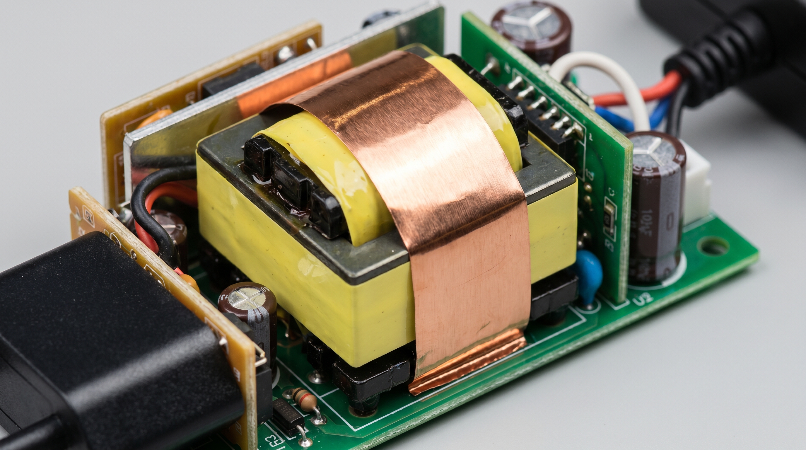
Why use copper foil inside transformers?
The switching transformer is a primary source of common-mode capacitive noise coupling. Wrapping an isolated copper foil shield between its windings blocks this electrical coupling path.
Think about it:
Diverting parasitic currents back to ground keeps your output rails clean.
- Insulate foil edges to prevent high-voltage electrical shorts.
- Connect to primary ground to provide a safe discharge path.
- Cover windings fully to ensure maximum electrostatic containment.
Key Takeaway: Adding internal metal shielding wraps traps high-frequency fields, keeping radiated energy bottled safely inside the adapter.
| Shielding Type | Shielding Material | Target Frequency Range | |
|---|---|---|---|
| Transformer Shield | Copper foil tape | 10 MHz to 100 MHz (Capacitive) | |
| Chassis Cage | Steel plate frame | Below 30 MHz (Magnetic) | |
| RF Absorber Sheet | Ferrite composite polymer | Above 150 MHz (High-frequency) |
Applying the correct shielding material to the corresponding field type is essential to pass stringent radiated testing.
Which parts resolve power adapter EMI and EMC?
Selecting the correct passive components is vital to developing a clean power system. A well-designed input filter acts as your ultimate defense against power adapter EMI and EMC conducted noise.
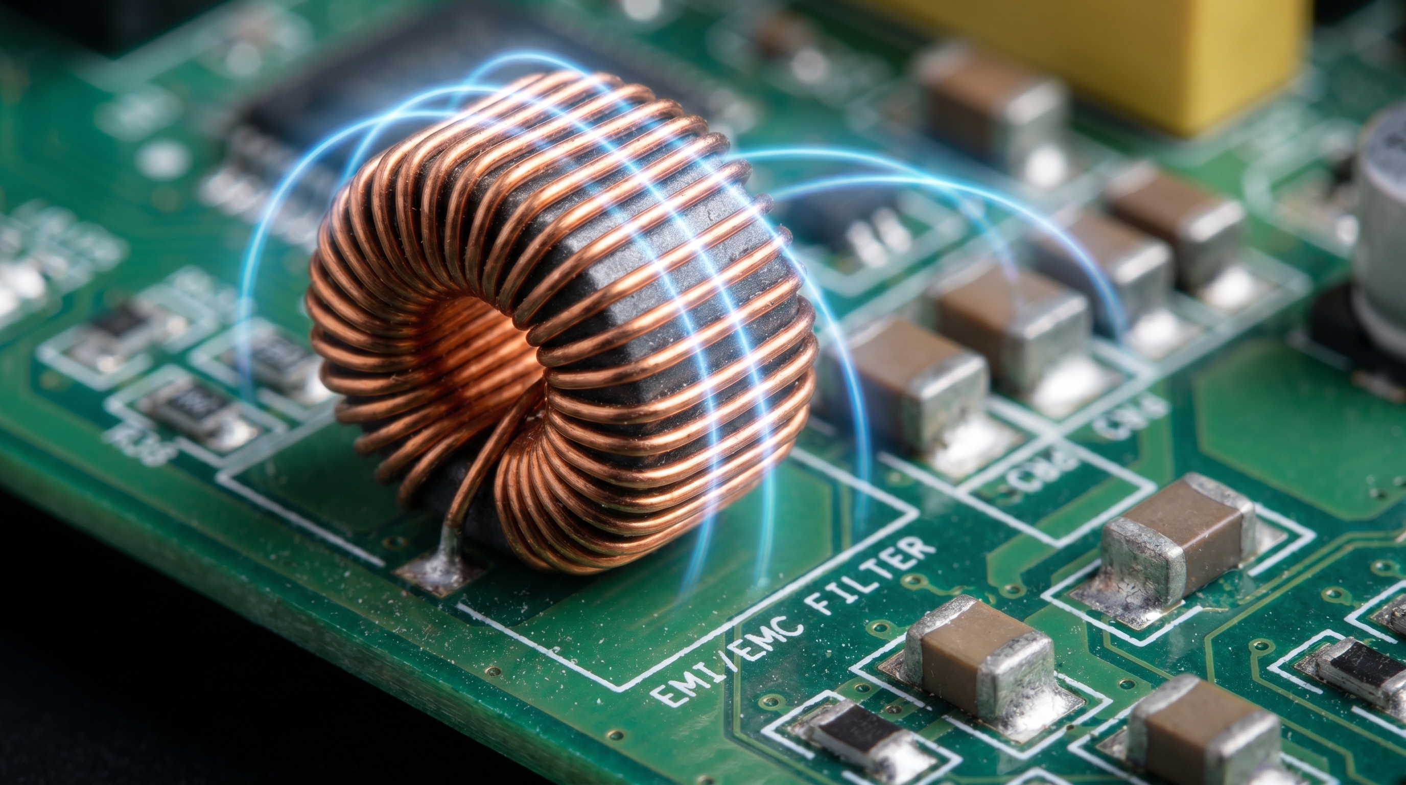
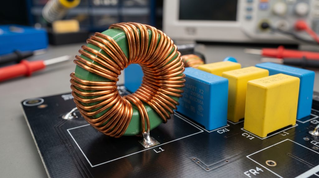
How do common-mode chokes block noise?
Common-mode chokes consist of dual windings wound onto a single magnetic toroidal core. They present high impedance to in-phase common-mode noise while letting differential currents flow.
Look:
They act like an impenetrable wall for common-mode power line noise.
- High magnetic permeability maximizes noise absorption at low frequencies.
- Matching physical windings cancels out opposing differential currents.
- Optimized core materials prevent saturation during high-load peaks.
Why are X and Y capacitors critical?
Safety-certified capacitors are placed at the power entry to filter out line noise. X-capacitors handle line-to-line noise, while Y-capacitors bypass line-to-ground noise.
Here is why:
Standard capacitors can fail dangerously if exposed to high-voltage surges.
- Use X-capacitors for suppression of differential line-to-neutral noise.
- Deploy Y-capacitors for suppression of common-mode line-to-ground noise.
- Limit leakage current to guarantee compliance with medical standards.
Key Takeaway: Combining passive common-mode chokes with safety capacitors creates a multi-stage filter that blocks conducted emissions.
| Component Type | Target Suppression Mode | Critical Design Parameter | |
|---|---|---|---|
| Common-Mode Choke | Common-mode (in-phase) noise | Impedance versus frequency curve | |
| X-Capacitor | Differential (line-to-line) noise | Safety classification rating | |
| Y-Capacitor | Common-mode (line-to-ground) noise | Maximum allowable leakage current |
Hardware developers must model filter responses to prevent components from resonating and amplifying switching harmonics.
What standards rule power adapter EMI and EMC?
Every global market legally mandates electromagnetic emissions and immunity verification. Sourcing power supplies pre-certified to power adapter EMI and EMC global rules prevents massive legal and commercial blockages.
What are the FCC Part 15 rules?
In North America, the Federal Communications Commission dictates strict emission rules. They categorize devices under Class A for industrial use or Class B for residential use.
Here is the catch:
Selling uncertified consumer electronics in the United States is illegal.
- Conducted test range spans from 150 kHz up to 30 MHz.
- Radiated test range scans frequencies up to 1 GHz.
- Class B limits are far more stringent than industrial limits.
What is the CISPR 32 global standard?
CISPR 32 is the international benchmark standard for multimedia hardware. It serves as the framework for European harmonized standards like EN 55032.
Let’s dive right in:
This standard ensures electronics can coexist globally without interfering.
- Harmonizes test setups so one test report covers global markets.
- Sets international limits for conducted and radiated emissions.
- Standardizes test equipment to ensure consistent laboratory results.
Key Takeaway: Selecting pre-certified power adapters with CE and FCC marks dramatically reduces your own product’s testing costs.
| Standard Code | Active Region | Focus Area | Equipment Classification | |
|---|---|---|---|---|
| FCC Part 15 | United States | Conducted & Radiated | Class A (Industrial) / Class B (Residential) | |
| CISPR 32 | International | Multimedia Emissions | Global limits harmonization | |
| EN 55032 | European Union | Emissions CE Mark | Harmonized European test limits |
Compliance officers must verify that test reports confirm Class B compliance to guarantee residential sales authorization.
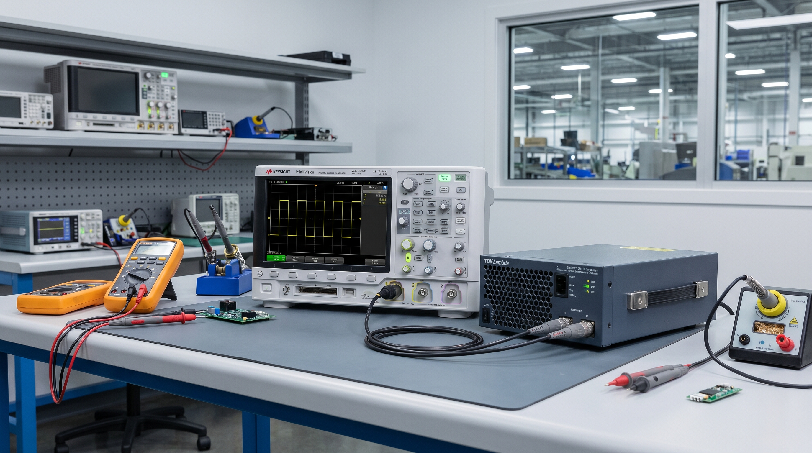
How do labs verify power adapter EMI and EMC?
Earning regulatory approval requires your product to pass formal laboratory testing. Measuring power adapter EMI and EMC performance requires highly calibrated instrumentation and specialized rooms.
What is conducted emissions testing?
Conducted emission testing measures the electrical noise your adapter injects back into the grid. A Line Impedance Stabilization Network (LISN) isolates this noise from grid interference.
Look:
The LISN prevents grid-side noise from contaminating your test data.
- Clean reference impedance ensures consistent testing across global labs.
- RF signal isolation routes noise straight to the analyzer.
- Overload protection guards sensitive measuring inputs from surges.
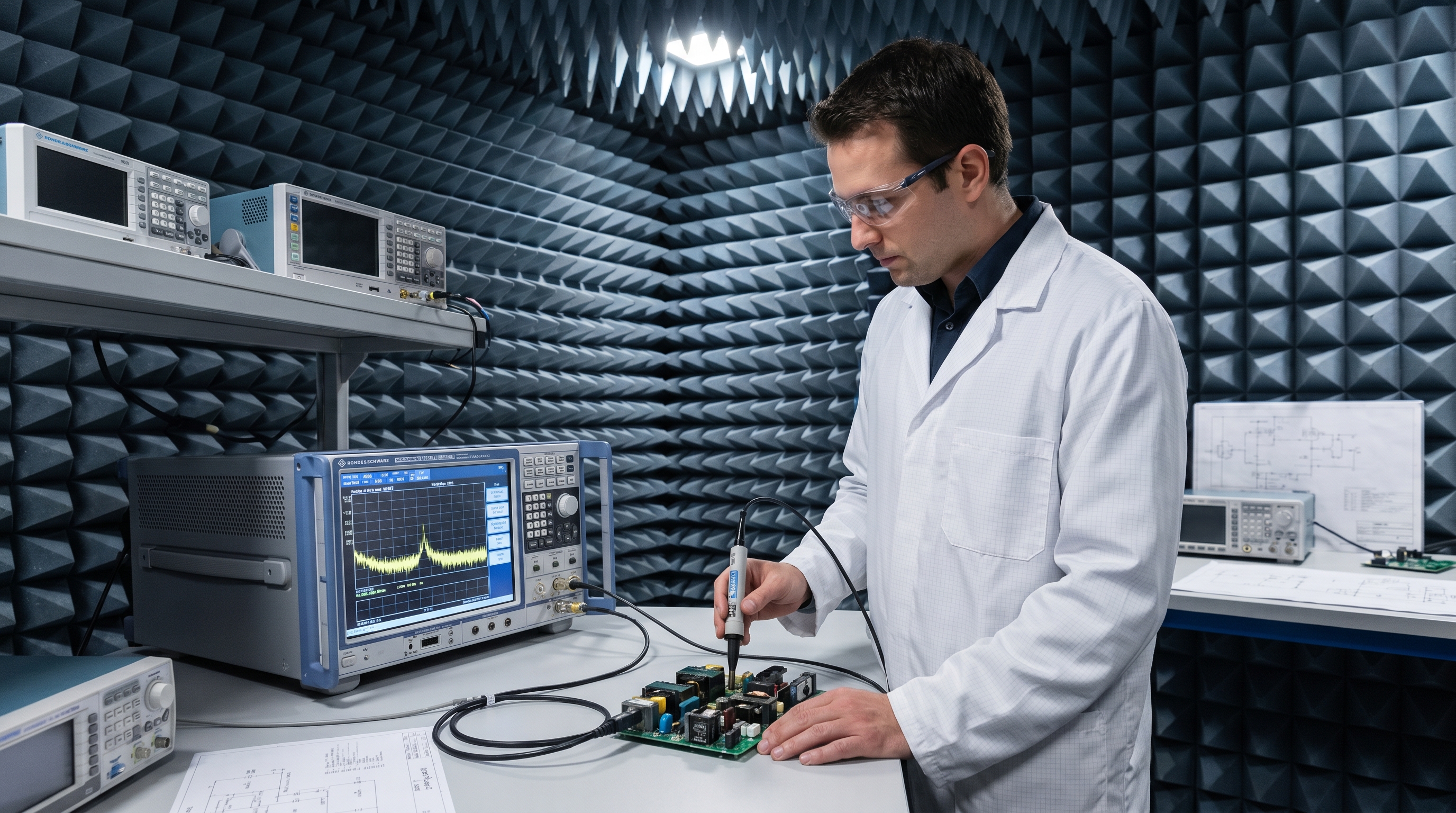
How do anechoic chambers work?
Radiated emissions are measured inside large, RF-shielded anechoic chambers. These rooms are lined with blue foam pyramids that absorb radio waves, preventing reflections.
Here is why:
Reflections inside a standard room cause constructive interference, giving false failures.
- Standardized turntable rotation scans for noise from all 360 degrees.
- Automated antenna masts scan heights from 1 to 4 meters.
- Metallic outer shielding blocks ambient local FM and cellular signals.
Key Takeaway: Conducting early pre-compliance sweeps in your lab avoids highly expensive failures during final formal testing.
| Test Phase | Frequency Range | Key Laboratory Equipment | |
|---|---|---|---|
| Conducted Emission | 150 kHz to 30 MHz | LISN and EMI Signal Receiver | |
| Radiated Emission | 30 MHz to 1 GHz+ | Anechoic Chamber and Antenna | |
| Surge Immunity | High-energy pulse | High-voltage Surge Simulator |
Hardware designers should complete near-field probe scans prior to booking expensive, formal anechoic chamber sessions.
Why do factories need power adapter EMI and EMC?

Industrial environments are filled with automated machinery and high-power switches that generate immense electrical noise. Standard power units will fail in these setups, making rugged power adapter EMI and EMC designs crucial.
How harsh is factory power grid noise?
Industrial power grids suffer from frequent, massive voltage spikes and strong magnetic fields. Heavy electric motors turning on and off inject severe surges back into power lines.
Think about it:
A standard consumer adapter would burn out within days in this environment.
- High-energy surges occur when grid switches divert power loads.
- Fast transient bursts leak from heavy solenoids and motor contactors.
- Strong inductive fields radiate directly from high-power machinery.
Can noise trigger factory downtime?
If your integrated adapter lacks robust immunity, incoming noise can crash sensitive programmable logic controllers. A single system reset on a robot line can cost thousands of dollars per minute.
But wait, there’s more:
Continuous electrical noise also degrades the accuracy of manufacturing sensors.
- Thick surge absorbers clamp incoming high-voltage line surges safely.
- Heavy filter chokes block incoming high-frequency line interference.
- Wide input tolerances prevent system resets during grid voltage sags.
Key Takeaway: Industrial systems demand high-immunity power supplies that survive hostile power grids while shielding sensitive controllers.
| Performance Metric | Consumer Adapter Standard | Industrial Adapter Standard | |
|---|---|---|---|
| Surge Immunity | 1 kV Line-to-Line | 2 kV to 4 kV minimum | |
| Radiated RF Immunity | 3 V/m field strength | 10 V/m field strength minimum | |
| Operating Temp Range | 0°C to 40°C | -40°C to 85°C extended |
Procurement officers must specify robust industrial-grade immunity ratings when sourcing power modules for automated factories.
How to optimize power adapter EMI and EMC design?

Resolving emission issues requires integrating noise suppression directly into your CAD board layout. Designing for power adapter EMI and EMC compliance from day one is far more effective than trying to patch failures late.
How to optimize CAD ground planes?
A solid, continuous ground plane provides a low-impedance path for return currents. Keeping return currents close to their active trace lines cancels out magnetic fields.
Look:
This close routing drastically reduces your PCB’s radiated antenna loop area.
- Avoid ground trace splits that force return currents to loop.
- Place decoupling caps directly adjacent to chip power pins.
- Separate switching zones physically from sensitive analog circuitry.
Why partner with an OEM manufacturer?
Designing a compliant, high-efficiency power supply from scratch is incredibly complex and risky. Partnering with an experienced manufacturer allows you to deploy pre-tested designs.
Here is why:
They already possess certified platforms that can be easily customized.
- Deploy pre-tested layouts that have already passed laboratory sweeps.
- Access custom inductors tuned to your exact circuit frequencies.
- Leverage global certifications to bypass expensive laboratory steps.
Key Takeaway: Optimizing your PCB ground routing and partnering with certified factories is the fastest path to achieving market approval.
| Design Focus | Physical Action | Technical Benefit | |
|---|---|---|---|
| Switching Loops | Keep trace loop areas compact | Lowers radiated magnetic field strength | |
| Grounding Layout | Run continuous ground planes | Minimizes common-mode return impedance | |
| Gate Drive Speed | Install series gate resistors | Suppresses high-frequency switching harmonics |
Layout designers must balance active switching speeds with thermal dissipation limits to achieve optimal efficiency.
Conclusion
Navigating power adapter EMI and EMC requirements is essential to launching a reliable, legally compliant electronic product. By implementing robust filter networks, tight ground plane designs, and effective physical shielding, you can suppress noise issues before they compromise your product’s success.
If you are currently facing certification delays or require a high-reliability, globally certified power supply, our engineering team is here to help. We invite you to contact us today to discuss your technical specifications and request free engineering samples.
Frequently Asked Questions
Can I use an unshielded power adapter for medical projects?
Absolutely not. Medical systems are governed by strict safety and immunity laws, meaning you must utilize highly shielded, medical-grade power supplies to prevent interfering with life-support telemetry.
What is the best way to trace high-frequency radiation?
Use near-field probes connected to a spectrum analyzer directly over your adapter’s circuit board. This allows you to pinpoint the exact traces, transistors, or transformer pins that are emitting high frequencies.
Can custom shields fix an already failing design?
Yes, but partially. Applying metal shields can resolve failing radiated emission results late in a development cycle, but they cannot resolve conducted emissions, which require line filters and chokes.
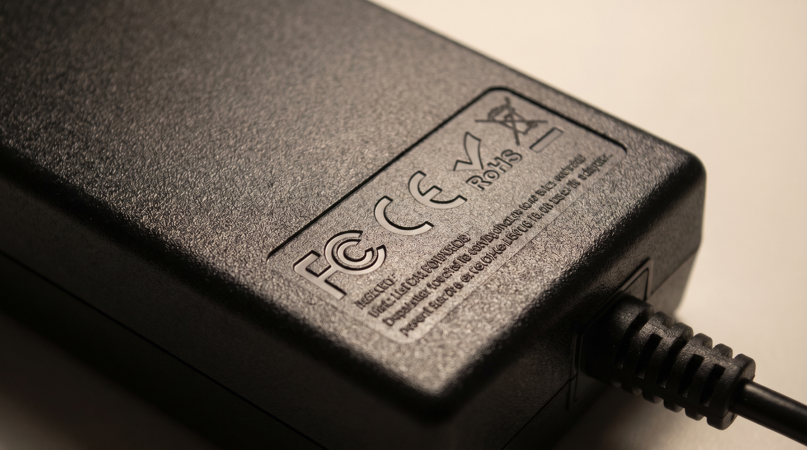
How do I verify if my adapter is truly FCC certified?
Look up the FCC ID. You can easily search the manufacturer’s unique FCC identification number directly on the official FCC Office of Engineering and Technology database to verify certificate validity.
What is the most cost-effective EMI suppression part?
A ferrite bead. Clamping a simple ferrite bead onto the DC output cable is the most cost-effective method to suppress high-frequency radiated noise without redesigning your internal circuit board.