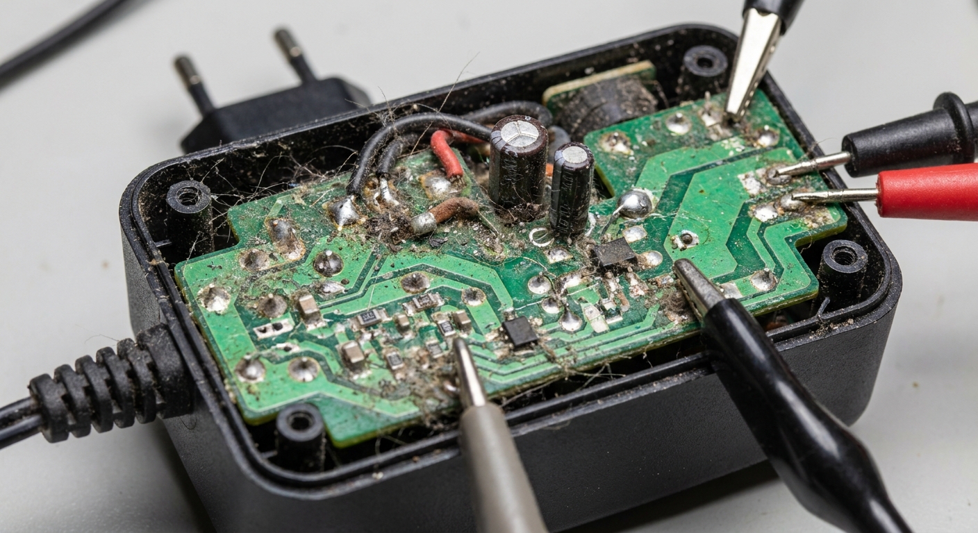
Creepage distance in power supplies is the shortest path between two conductive parts measured along the surface of the insulating material. Designing high-density power converters often forces engineers to cram high-voltage components into extremely tight spaces, leading to physical clearance bottlenecks. If you ignore these spacing limits, minor environmental dust, humidity, or condensation will create conductive tracking paths along the board surface, resulting in catastrophic short circuits, fires, or failed safety audits. Properly implementing the creepage distance in power supplies acts as a critical safety defense mechanism, ensuring robust dielectric isolation even under the most demanding operating conditions.
Defining Creepage Distance in Power Supplies
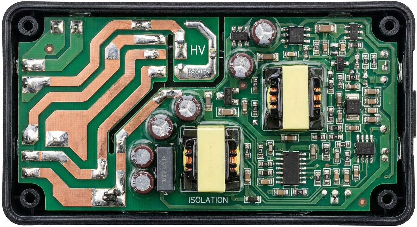
Defining this parameter correctly requires measuring the physical distance along the surface of an insulating board rather than through the air. This distinction is critical when engineering a high-voltage power adapter for energy storage systems where surface pathways are vulnerable to degradation. Over time, continuous voltage bias across these pathways can compromise safety barriers if they are not sized with precision.
How does surface tracking affect isolation safety?
If you neglect surface degradation, voltage stress will eventually break down your dielectric barrier.
Let’s dive in:
- Carbon Track Formation: Electric current degrades the PCB resin, leaving a permanent carbonized pathway.
- Increased Leakage: Once tracking begins, leakage current rises exponentially across the board.
- Component Damage: This breakdown eventually leads to catastrophic component failures or fires.
Key Takeaway: Correctly defining and sizing your surface spacing prevents localized tracking and safeguards high-voltage operations.
| Parameter | Measurement Path | Key Threat Addressed | Mitigation Strategy | |
|---|---|---|---|---|
| Creepage | Surface contour | Electrical tracking | Physical isolation slots |
This structural separation ensures that high-voltage pathways remain isolated even under severe operational stress.
Why Creepage Distance in Power Supplies Matters
Maintaining safety margins on the PCB surface is the only way to prevent hazardous electrical tracking and potential shock risks to the end user. This baseline safety plays an indispensable role in developing a robust power adapter for energy storage systems where voltages routinely exceed hundreds of volts. Failing to prioritize these surface barriers during layout compromises the entire structural safety of your hardware.
How do adequate surface paths prevent electrical shocks?
When you manage high-voltage lines, you must provide a physical barrier that prevents current from bridging to touchable surfaces.
Think about this:
- Galvanic Protection: Adequate spacing maintains complete separation between the primary AC input and the secondary DC output.
- Thermal Control: Keeping high-voltage traces spaced apart prevents thermal runaway across the FR-4 substrate.
- User Isolation: Reliable barriers guarantee that terminal voltages remain safe for operators to touch.
Key Takeaway: Maintaining robust spacing limits prevents high-voltage leakage from reaching low-voltage user interfaces.
| Hazard | Root Cause | Safety Consequence | Preventive Strategy | |
|---|---|---|---|---|
| Shock | Surface tracking | User exposure to high voltage | Double/reinforced insulation |
Using robust physical spacing isolates sensitive outputs from dangerous input transients.
Creepage Distance in Power Supplies vs Clearance
The primary difference lies in the medium of travel: creepage is measured along the surface, whereas clearance is measured through free air. When optimizing a power adapter for energy storage systems , you must design for both mechanisms independently to protect against distinct failure modes. While clearance prevents instant arcing through the air, surface pathways protect against slow degradation.
When should you focus on surface paths over air gaps?
You must prioritize surface pathways whenever your system is deployed in humid or dusty environments.
Here is the catch:
- Dust Accumulation: Air gaps do not collect contaminants, but board surfaces gather particles that facilitate tracking.
- Condensation Cycles: Moisture films only form on solid surfaces, drastically dropping surface resistivity.
- Space Limits: You can easily increase surface paths by routing slots without altering component positions.
Key Takeaway: Designing physical slots on the PCB allows you to extend creepage without increasing the overall board width.
| Metric | Travel Medium | Failure Mode | Key Variable | |
|---|---|---|---|---|
| Creepage | Solid surface | Slow tracking / carbonization | Material CTI, pollution degree | |
| Clearance | Free air | Instant arcing | Air pressure, altitude |
Balancing these two distinct dimensions allows you to optimize both packaging density and safety compliance simultaneously.
IEC Standards for Creepage Distance in Power Supplies
International standards establish specific, legally mandated spacing dimensions based on operating voltage, material properties, and environmental conditions. If you are validating a power adapter for energy storage systems, standard rules such as IEC 62368-1 outline the precise millimetric requirements you must meet. Skipping these mandatory steps during layout will inevitably cause safety lab failures.
What are the core requirements of IEC 62368-1?
You must classify your power supply into the correct energy source category to determine its insulation requirements.
The reality is simple:
- Basic Insulation: Provides a single level of protection against shock under normal operating conditions.
- Reinforced Insulation: Delivers double the protection, ensuring safety even during a single-fault component breakdown.
- Pollution Class: Most consumer and industrial environments require planning for standard Pollution Degree 2 limits.
Key Takeaway: Complying with IEC 62368-1 guarantees that your hardware meets global legal and safety parameters.
| Standard | Target Sector | Basic Requirement | Reinforced Requirement | |
|---|---|---|---|---|
| IEC 62368-1 | Consumer / IT | Single insulation layer | Double / reinforced isolation |
This standardized framework ensures uniform safety margins across diverse electronics markets.
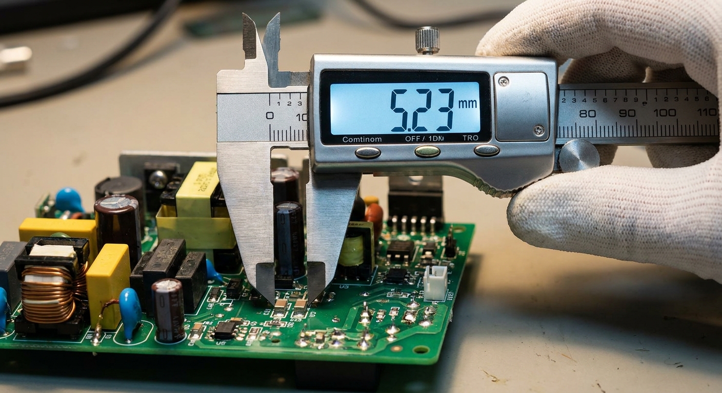
Calculating Creepage Distance in Power Supplies
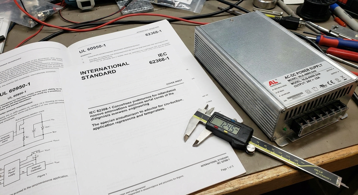
Calculating this spacing requires identifying the RMS working voltage, the environment’s pollution degree, and the PCB material’s tracking resistance. When developing a power adapter for energy storage systems , you must first measure the continuous peak and average voltage waves across your isolation barrier. Failing to verify these three primary parameters makes accurate compliance mapping impossible.
How do you perform the step-by-step calculation?
You need to follow a systematic lookup process using the safety tables provided by your target regulatory body.
But wait, there’s more:
- Measure Voltage: Capture the peak and RMS operating voltages using a differential probe on your testbench.
- Identify Material: Check your laminate datasheet to determine its Comparative Tracking Index (CTI) rating.
- Lookup Spacing: Map these parameters to the correct safety table to find the minimum distance required.
Key Takeaway: Systematic calculations eliminate layout guesswork, protecting your designs from costly safety laboratory failures.
| Step | Parameter | Input Source | Final Output | |
|---|---|---|---|---|
| 1 | Working Voltage | Waveform analysis | RMS/Peak Value | |
| 2 | CTI Group | Substrate datasheet | Material class (I-IIIb) |
By systematically checking these variables, you prevent accidental insulation failures during high-power runtime cycles.
Environmental Impact on Creepage Distance in Power Supplies
Ambient environmental conditions like humidity, dust, and altitude directly dictate how quickly the surface insulation degrades over time. When your power adapter for energy storage systems is deployed in outdoor or industrial cabinets, it experiences harsh conditions that accelerate tracking. Designing for clean lab conditions rather than real-world operating environments is a recipe for field failure.
How does moisture change surface conductivity?
You must understand how moisture interacts with microscopic dust particles on your PCB surface.
Let’s dive in:
- Condensation Effects: Rapid cooling cycles create micro-droplets of water across your isolation barriers.
- Ionic Dissolution: These water drops dissolve surface salts, creating a highly conductive electrolyte pathway.
- Tracking Breakdown: The resulting leakage current heats the surface, forming permanent carbon channels.
Key Takeaway: Accounting for ambient humidity prevents localized tracking from permanently destroying your PCB’s safety isolation.
| Condition | Operational Risk | Spacing Impact | Recommended Protection | |
|---|---|---|---|---|
| High Humidity | Electrolytic conduction | Demands wider spacing | Conformal coating / potting |
Adapting layout parameters to handle humidity prevents environmental field failures and protects system integrity.
Materials and Creepage Distance in Power Supplies
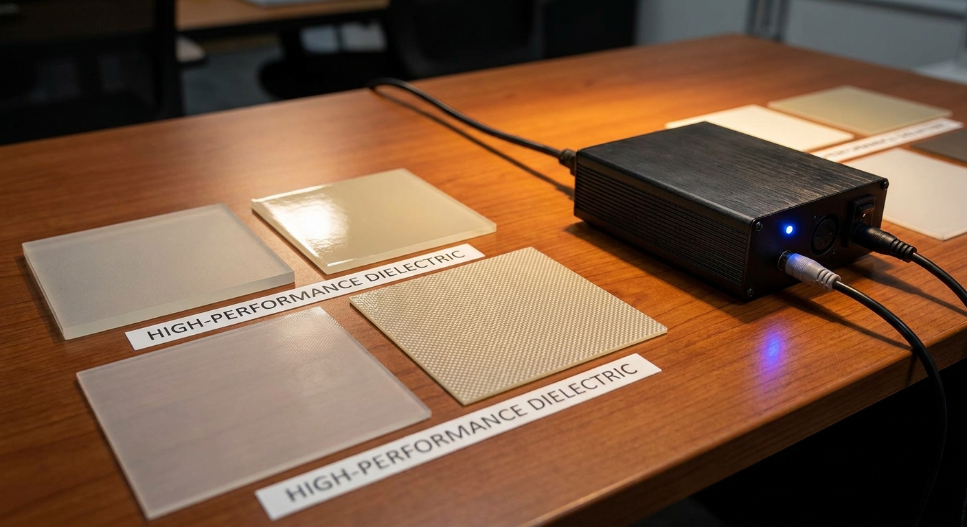
Substrate material properties, quantified by the Comparative Tracking Index (CTI), define how resistant the board is to forming carbonized paths. When specifying materials for a power adapter for energy storage systems , choosing a substrate with a high CTI allows you to safely compress your spacing. Using standard low-cost materials, however, requires significantly larger physical layout footprints to pass safety guidelines.
How does the CTI rating impact your layout footprint?
You can save significant board real estate simply by upgrading your substrate material group.
Here’s the deal:
- Group I Substrates: These premium laminates (CTI ≥ 600V) offer exceptional tracking resistance, minimizing required spacing.
- Group IIIa Substrates: Standard FR-4 (175V ≤ CTI < 400V) requires significantly larger spacing distances to comply.
- Material Selection: Matching your substrate selection to operating voltages keeps your physical footprint compact.
Key Takeaway: High-CTI materials allow you to shrink your layout without compromising on electrical tracking protection.
| Material Group | CTI Range | Spacing Requirement | Cost Impact | |
|---|---|---|---|---|
| Group I | ≥ 600 V | Minimal | Higher material cost | |
| Group IIIa/b | < 400 V | Standard / Maximum | Standard cost |
Upgrading your dielectric material class provides a reliable path to reducing board size safely.
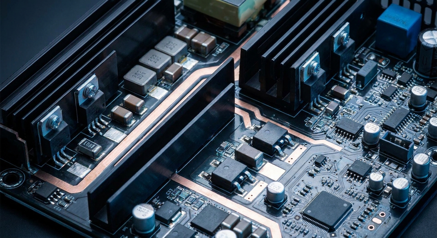
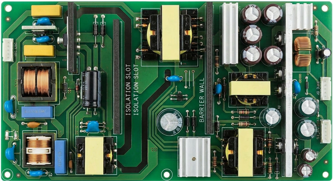
Optimizing Creepage Distance in Power Supplies on PCBs
Optimizing this parameter requires implementing physical PCB modifications, such as milled slots, to block surface-level electrical conduction. For a compact power adapter for energy storage systems, routing these physical slots is often the only way to meet target spacing rules. Integrating these mechanical design features early in the layout process prevents costly downstream board revisions.
Can you use milled slots to increase spacing?
You can easily double your effective isolation pathway by cutting physical channels through the board laminate.
Think about this:
- Air Interruption: Cutting a slot converts a solid surface path into an airborne path.
- Width Rules: Ensure your slots are at least 1 mm wide to prevent moisture bridging.
- Pin Spacing: Staggering terminal layout pins on high-voltage components naturally expands your spacing.
Key Takeaway: Milled isolation slots are the most cost-effective mechanical technique for expanding spacing on tight layouts.
| Technique | Layout Benefit | Tooling Cost | Structural Risk | |
|---|---|---|---|---|
| PCB Slotting | Converts path to clearance | Minimal | May weaken board structure |
Combining milled slots with smart component positioning maximizes safety inside high-density enclosures.
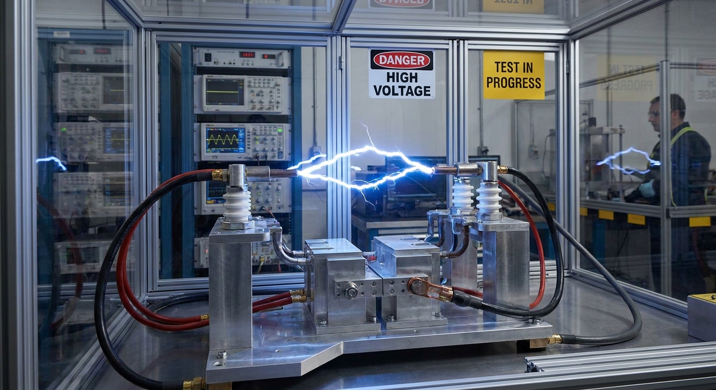
Testing Creepage Distance in Power Supplies for Safety
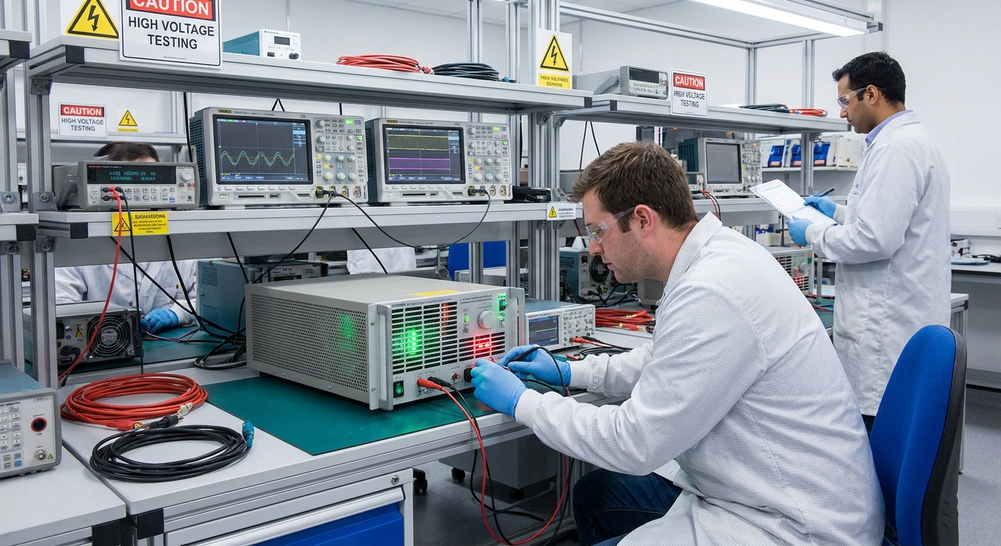
Verifying compliance requires running physical laboratory tests, such as high-potential (hipot) testing and microscopic geometric inspections, on production units. When certifying a power adapter for energy storage systems , quality control must prove that real-world assemblies match design files. Even minor assembly variations can easily bridge a borderline isolation pathway.
Does high-potential testing catch surface issues?
You must understand that a standard hipot test may not detect a borderline surface tracking issue.
The reality is simple:
- Hipot Limitations: Hipot testing mainly catches immediate air gaps or dielectric breakdowns, not future surface decay.
- Optical Checks: You must use high-precision microscopes to physically measure layout dimensions.
- Environmental Testing: Running continuous humidity cycles accelerates potential tracking failures under stress.
Key Takeaway: A comprehensive testing protocol must pair high-voltage hipot testing with visual geometric inspections.
| Test Protocol | Equipment Used | Primary Detection Focus | Compliance Standard | |
|---|---|---|---|---|
| Hipot | Hipot Tester | Instant dielectric breakdown | IEC 62368-1 | |
| Optical Measurement | 3D Measuring Scope | Spacing layout dimensions | Mechanical layout |
Using multiple testing methodologies guarantees that potential field failures are caught during the factory phase.
Fixing Creepage Distance in Power Supplies Design Issues
Resolving insulation design challenges requires correcting 3D layout interference, optimizing mounting hardware, and applying protective barrier walls. In a typical power adapter for energy storage systems, mechanical components like mounting screws or heatsinks often create unintended electrical paths. Evaluating your spacing solely in a flat 2D layout editor leads to missing these critical physical interference points.
How do you eliminate common 3D layout errors?
You need to audit your entire assembly in a 3D mechanical modeling environment.
But wait, there’s more:
- Hardware Clearances: Verify that metal screws and standoffs do not cut into your keepout areas.
- Plastic Ribs: Design integrated barrier walls into your plastic housing to physically block pathways.
- Conformal Coating: Apply protective coatings using automated sprayers to avoid pinholes and air bubbles.
Key Takeaway: Auditing layouts in 3D catches mechanical interference points before tooling and production begin.
| Design Issue | Root Cause | Preventive Strategy | Compliance Verification | |
|---|---|---|---|---|
| Metal Screw Bypass | Incorrect keepout zone | 3D modeling review | Clearance measurement |
Catching these structural errors during layout keeps your production schedules on track and prevents costly redesigns.
Engineering Safe and Compliant Power Infrastructures
Integrating precise isolation spacing into high-density electronics remains a fundamental pillar of modern power engineering. From high-power grid equipment to a robust power adapter for energy storage systems, managing physical spacing along PCB surfaces prevents tracking failures, guarantees safety compliance, and eliminates costly redesign delays. At Fuyuang, we deliver certified, reliable power adapters engineered to perform flawlessly under severe conditions. If you are ready to design next-generation electronics with guaranteed compliance, contact us today to consult with our technical specialists.
Safety Isolation Frequently Asked Questions
Can I use standard FR-4 for high-voltage power designs?
Yes, but you must carefully check its Comparative Tracking Index (CTI) first. Standard FR-4 typically falls into Material Group IIIa, which has low tracking resistance and requires wider spacing paths. For compact power supplies, upgrading to a high-CTI substrate allows you to safely shrink your layout.
What’s the best way to extend surface pathways on a crowded PCB?
Milling isolation slots directly between high-voltage pads is the most effective technique. Cutting an air slot breaks the continuous surface path, converting a surface-bound calculation into an air-gap calculation. This allows you to maintain safe isolation without moving your components.
Does conformal coating eliminate safety spacing requirements?
No, conformal coating does not replace proper layout spacing. While a high-quality coating acts as a barrier against moisture and dust, safety agencies do not treat it as a perfect isolator unless it meets strict thickness and application requirements. Any pinholes or air bubbles in the coating will compromise your protection.
Can high altitude affect safety limits in my power supply?
Yes, altitude has a major impact on safety spacing parameters. At altitudes above 2000 meters, the thinning air has a lower breakdown voltage, which makes air arcing much more likely. You must apply standard scaling multipliers to both clearance and surface spacing to ensure high-altitude safety.
How do I know if my layout requires basic or reinforced insulation?
The isolation level is determined by the safety category of the product and whether users can touch the output terminals. Basic insulation offers a single layer of protection, whereas reinforced insulation delivers dual protection to survive single-component failures. Consult standard IEC tables to verify your target safety architecture.